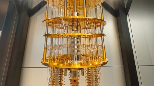

IBM is committing $1 billion in cash and intellectual property to launch Anderon, described as the world’s first pure-play quantum wafer foundry, as part of a broader $10 billion quantum computing investment plan. The move shifts IBM from primarily building its own quantum systems to also supplying the specialized wafers that others will need to manufacture quantum chips at scale. It signals that quantum hardware is moving from bespoke lab projects toward an industrial supply chain with dedicated factories, long-term roadmaps, and national policy support.
How IBM’s quantum strategy expanded to a dedicated wafer foundry
IBM has laid out a multiyear roadmap that commits more than $10 billion to quantum computing, including hardware, software, and ecosystem development, with the goal of progressing from current systems to the world’s first fault tolerant quantum computers. The company framed this long-term plan as a way to fund everything from today’s processors to the future generations needed for error corrected machines, according to its quantum roadmap. Within that broader commitment, Anderon represents a focused bet that the bottleneck for quantum progress will increasingly sit in manufacturing capacity rather than just in lab breakthroughs.
Structured as a pure-play quantum wafer foundry, Anderon is designed to produce wafers for quantum devices as its primary business instead of bundling that work inside a larger internal product group. IBM is putting $1 billion in cash into the venture and pairing that with a significant transfer of intellectual property, including process recipes and design know-how accumulated over years of building superconducting quantum chips. By separating the wafer operation from its system integration teams, IBM is signaling that it expects a broader market of external customers that will want access to advanced quantum wafers without buying full IBM systems.
The new foundry is also tied to a public sector push to establish domestic quantum manufacturing. IBM and the U.S. Department of Commerce jointly announced plans for what they describe as America’s first purpose built quantum foundry, with the federal side considering a proposed $1 billion CHIPS and Science Act award to support the project. That plan, outlined in a joint IBM and Commerce announcement, positions Anderon as a key asset in national semiconductor and quantum policy.
Further details from the same initiative describe a facility that will focus on wafer-level fabrication for quantum processors, supported by the proposed $1 billion CHIPS funding and IBM’s own capital and IP contributions. Reporting on the program highlights that this would be a purpose built quantum foundry located in the United States, intended to serve both IBM and outside customers as part of a broader CHIPS award proposal. The alignment between IBM’s $10 billion quantum roadmap and this public funding proposal has effectively created the financial and policy foundation for Anderon to launch as a specialized manufacturing hub.
Why a pure-play quantum wafer foundry is emerging now
IBM’s decision to carve out a dedicated quantum wafer foundry reflects a shift in where the hardest problems in quantum computing now lie. Early progress depended on demonstrating that qubits could be controlled, entangled, and read out with reasonable fidelity. Today, the challenge is building systems with enough high quality qubits, connected in the right topologies, to support error correction and practical workloads. Reaching that stage requires repeatable, high yield manufacturing on wafers, not just handcrafted chips from a research clean room.
By pouring $1 billion in cash and IP into Anderon, IBM is betting that scaling quantum hardware will look more like the evolution of classical semiconductors, where dedicated foundries such as TSMC became the backbone of the industry. A pure-play structure makes it easier for Anderon to serve multiple quantum hardware designers, including startups and research institutions, without forcing them into IBM’s system architecture. It also lets IBM monetize its process knowledge as a platform, not only as finished machines.
National industrial policy is also shaping the timing. The proposed $1 billion CHIPS award for the quantum foundry shows that U.S. policymakers see quantum manufacturing as a strategic capability, similar to advanced logic and memory fabs. Combining federal support with IBM’s $10 billion quantum program concentrates enough capital to justify a facility that would be uneconomical as a small, single-customer line. That public private structure mirrors how traditional semiconductor megafabs have often been financed in regions that want to anchor high value manufacturing.
From a market perspective, Anderon arrives as more companies and labs move from proof-of-concept qubit devices toward application-oriented prototypes. Financial institutions are experimenting with quantum algorithms for portfolio optimization, automotive companies such as Volkswagen and BMW have tested quantum approaches to traffic flow and materials discovery, and pharmaceutical firms are exploring quantum chemistry simulations. None of these use cases will reach meaningful scale without access to more capable and reliable hardware. A foundry that can supply wafers for multiple quantum modalities, particularly superconducting qubits, could accelerate that transition by giving hardware designers a predictable manufacturing partner.
There is also a geopolitical dimension. Several countries have signaled ambitions in quantum technologies, with significant investments in Europe and Asia. A U.S.-based pure-play quantum wafer foundry supported by both IBM and the Department of Commerce positions the United States to retain a central role in the supply chain for quantum processors. That matters not only for economic reasons but also for security concerns, since some quantum applications intersect with cryptography, defense analysis, and critical infrastructure modeling.
How Anderon could reshape IBM’s roadmap and the broader quantum ecosystem
Within IBM’s own portfolio, Anderon is likely to become the manufacturing backbone for the company’s future quantum processors. As IBM pursues its plan to progress from current devices to fault tolerant systems backed by its more than $10 billion quantum commitment, it will need a steady pipeline of wafers that support larger qubit counts, better coherence times, and more complex interconnects. A dedicated foundry gives IBM tighter control over process variation and capacity planning, which are essential for building multi-generation hardware roadmaps.
For the wider ecosystem, Anderon could function as a neutral infrastructure layer that lowers the barrier to entry for quantum hardware innovation. Startups that design new qubit layouts or control schemes often struggle to secure time on advanced fabrication lines that understand quantum requirements. If Anderon offers multi project wafer runs, process design kits tailored to quantum devices, and engineering support, it could become a default choice for emerging players that lack the resources to build their own fabs. That would echo the role that specialized foundries played in enabling the fabless semiconductor model in classical computing.
The interplay between Anderon and the proposed CHIPS funding will shape how accessible the foundry is to non IBM customers. If the facility is structured to meet both IBM’s internal demand and external projects that align with U.S. research and industrial goals, then universities, national labs, and startups could gain a path from lab prototypes to production scale wafers. That would help translate government spending on quantum research into tangible hardware platforms that industry can adopt.
There are, however, open questions that will determine how transformative Anderon becomes. Pricing and access policies will influence whether smaller companies can afford to use the foundry. The range of supported materials and qubit types will decide if Anderon is primarily a superconducting qubit factory or a more flexible platform that can handle alternative approaches. Integration with packaging, cryogenic control electronics, and system assembly will also matter, since wafers are only one part of a working quantum computer.
For IBM, success will be measured not only by wafer output but by whether Anderon helps the company reach fault tolerant systems on the schedule laid out in its quantum roadmap. If the foundry can consistently deliver higher yield and more advanced wafers, IBM’s system teams will have a stronger foundation for building large scale machines and for offering cloud access to those systems. That, in turn, would reinforce IBM’s position as both a technology leader and a key supplier in the emerging quantum industry.