
Ultra-thin electronics promise faster chips, flexible displays and ultra-efficient power devices, but a single invisible flaw in an insulating layer can quietly doom an entire component. A new method developed in the United States to spot those hidden defects before they cause failures could shift how chipmakers and device designers qualify their most delicate materials. Rather than relying on trial and error, engineers may soon have a practical way to see the weak spots inside atomically thin insulators and design around them.
The work centers on a strategic material used across cutting-edge electronics and energy systems, where tiny charge pockets can trigger breakdown, power loss and unpredictable behavior. By turning those invisible traps into a visible electrical signal, the technique opens a path to more reliable ultra-thin components, from next-generation processors to high-voltage switches and quantum devices.
Why hidden defects are a big problem for atomically thin materials
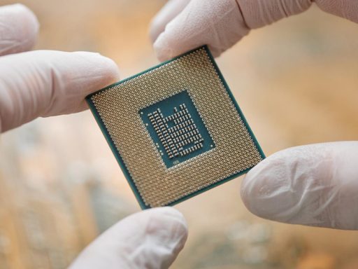
Modern ultra-thin electronics often stack layers only a few atoms thick, which makes them extremely sensitive to any microscopic imperfection. Hexagonal boron nitride, commonly called hBN, is one of the most important of these layers because it acts as an electrical insulator between active components while remaining atomically flat. Researchers at Rice University report that hidden defects inside hBN behave like tiny charge pockets that weaken insulation, so the same piece of material can start leaking electricity at much lower voltages than expected and fail unpredictably in real devices. That vulnerability is especially serious in power electronics and high-density chips, where designers push voltages and electric fields close to the limits of the material.
Traditional inspection tools struggle with this problem because the defects are effectively invisible. Under a regular optical microscope or even an atomic force microscope, the hBN flakes look uniform and clean, and standard electrical tests on simple structures often miss localized weak spots. As a result, manufacturers can ship devices that pass initial checks but later suffer breakdown, data corruption or efficiency losses once they are integrated into complex circuits. The new work, described in detail by Rice researchers, targets those elusive flaws directly rather than relying on indirect quality indicators.
The Rice University method that turns invisible traps into a visible signal
The core of the advance is a measurement strategy that forces hidden defects to reveal themselves through their electrical behavior. A team in the United States applies a controlled electric field across ultra-thin hBN layers and monitors how charges move and accumulate, effectively mapping where the material stores charge in places it should not. These subtle responses expose the tiny charge pockets that degrade insulation long before the layer reaches catastrophic breakdown. By comparing the behavior of many flakes, the researchers can distinguish between high-quality regions and sections riddled with problematic traps, which would be impossible to see with conventional imaging alone.
According to the detailed description of the work, the study focuses on hBN flakes that are transferred onto silicon and silicon dioxide wafers in a way that mimics real device fabrication. The researchers then track how the electrical response changes as the material is processed and stressed, revealing how manufacturing steps can introduce or amplify hidden defects. The method offers a practical path for process engineers to tune their recipes, since it gives direct feedback on which conditions create cleaner interfaces and which introduce dangerous charge pockets. One report notes that the same approach can be extended to other layered materials beyond hBN, which broadens its relevance for the wider family of two-dimensional electronics. That potential is highlighted in a segment that links the behavior of Yifeng Liu and to applications in additional stacked systems.
The researchers behind the breakthrough and how they tested it
The project is led by researchers at Rice University in the United States, where hBN and other two-dimensional materials have been a strategic focus. The study credits detailed experimental work carried out by Feb, Yifeng Liu and Tian Lang, with photography documenting the effort by Jorge Vidal at Rice University. Their work builds on a growing understanding that ultra-thin insulators can fail not because of obvious cracks or contamination, but because of subtle electronic traps that standard quality checks overlook. By designing experiments that deliberately stress the material and then observing how and where it begins to leak, the team created a template for future reliability studies on atomically thin stacks.
To validate the method, the researchers compared hBN flakes before and after transfer onto device substrates and then imaged the same regions after electrical testing. One account quotes Lee explaining that under a regular optical or atomic force microscope, the flakes appear unchanged, yet the new electrical imaging reveals dramatic differences in how charge accumulates after processing. That contrast confirms that the method is sensitive to real degradation in the material, not just measurement noise. The work is tied to a formal scientific report, referenced through the identifier 10.1021/acs.nanolett.5c06347, which anchors the findings in peer-reviewed data and provides a technical foundation for companies that may want to adopt the technique.
From lab technique to manufacturing tool for ultra-thin electronics
Industry interest in ultra-thin electronics spans flexible displays, wearable sensors, advanced processors and high-voltage switches, and all of these depend on reliable insulating layers a few atoms thick. Reports describe how researchers in the United States see the new method as a way to redefine quality control standards for those strategic materials, since it can flag dangerous defects before devices leave the factory. Instead of relying on simple pass or fail checks, manufacturers could grade material lots based on the density and severity of hidden charge pockets, then reserve the cleanest layers for the most demanding applications. That shift would directly improve yield and reduce the risk of field failures in sectors such as consumer electronics and energy infrastructure.
Coverage of the work emphasizes that ultra-thin electronics could become more efficient once engineers can systematically weed out flawed insulators. One analysis explains that by identifying where hBN starts to leak at lower voltages, designers can either discard weak material or adjust circuit layouts so that sensitive regions avoid those spots. That insight is framed as a way to boost performance without changing the underlying material system, since the same hBN can deliver higher reliability if it is screened and used intelligently. A detailed report on ultra-thin electronics notes that this kind of defect-aware design could help devices run closer to their theoretical limits without sacrificing safety margins.
What comes next for hBN and other layered materials
Although the current work focuses on hexagonal boron nitride, the underlying idea is general: any layered material that stores unwanted charge can, in principle, be screened with similar electrical imaging. Sources explain that the same approach could be applied to other two-dimensional semiconductors and insulators that are now being integrated into experimental chips, sensors and quantum components. That prospect matters for companies that are betting on stacked materials to extend Moore’s law, since they need reliable ways to qualify each layer in a complex stack. The researchers argue that by mapping out hidden traps before full device fabrication, engineers can avoid expensive late-stage failures and tune growth conditions for cleaner films.
There is also a broader institutional context behind the advance. The work connects back to Rice University’s broader investment in materials and applied physics, which is visible in the university’s public-facing presence at Rice University and its dedicated public affairs arm at pa.rice.edu. Outreach through technology-focused channels has amplified interest in the study, including coverage that highlights how scientists in the United States revealed an invisible defect in a strategic engineering material that could compromise chips and affect electronics and energy industries worldwide. One feature on US researchers stresses that the technique is not a niche laboratory curiosity but a candidate for integration into real production lines, where it could help ultra-thin electronics finally match their theoretical promise in the field.